Analog electronics
Adjustable-gain audio amplifier
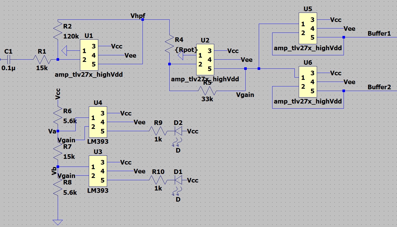
Designed, built, and measured an audio circuit with high-pass filtering, adjustable gain, output buffers, and LED level indicators.
Individual course project · EEL3111C · July 2026
My contribution
I designed the signal chain in LTspice, constructed the circuit, and compared its response with bench measurements using Analog Discovery. I checked DC-offset removal, gain, frequency response, and the output spectrum across the complete circuit.
Results & observations
The prototype removed the input DC offset and reproduced audio through powered speakers. Time-domain traces, a 10 Hz to 100 kHz frequency sweep, and spectral measurements documented its response, including residual noise and harmonics.
From a small signal to audible output
I combined a TLV272 active high-pass filter, adjustable inverting gain stage, two output buffers, and LM393 comparator indicators. The input capacitor removed a 0.5 V DC offset; the first-stage component values gave an estimated 106 Hz cutoff.
Build, simulate, measure
I compared LTspice behavior with the physical circuit using time-domain measurements, a frequency sweep, and an output spectrum. Both speaker channels received the same signal: this was dual mono, not independent stereo.
Gain, loading, and output quality
Connecting the stages meant checking gain, loading, bandwidth, and clipping together. The circuit produced audible output, while the measured spectrum showed residual noise and smaller harmonic components. Further distortion and noise testing would be needed to characterize audio fidelity.
Tools & methods
- LTspice
- Analog Discovery
- Op-amp design
- Active filters
- Signal buffering
- Comparator circuits
- Frequency response
- Spectrum analysis
- Bench testing